SÜSS MicroTec SE, a leading supplier of equipment and process solutions for the semiconductor industry, paves the way for Sy&Se’s novel low-temperature field-assisted bonding technology called Impulse Current Bonding. The technology is based on a major scientific discovery and will be made available on both manual and automatic wafer bonder systems.
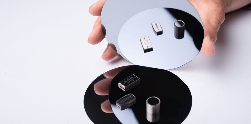
Impulse Current Bonding (ICB) combines the robustness of Anodic Bonding with the material versatility of other, more complex bonding methods. It allows for bonding of materials with different coefficients of thermal expansion, such as glass to metals, semi-metals, and ceramics. In addition, silicon to sapphire bonding confirms the potential for next-generation products as it is the first demonstration of an alkali-free field-assisted bonding. Compared to Anodic Bonding, the impulse current causes a higher interatomic diffusion at the material interface which leads to a strong and durable bond at lower temperatures and shorter process times.
Stefan Lutter, Business Unit Manager for SUSS MicroTec’s Bonder products, considers ICB a groundbreaking technology: “Impulse Current Bonding is a truly innovative approach that can be adapted to many different material systems and therefore opens up a broad range of new opportunities in the market. We are proud to be the exclusive partner of Sy&Se to deploy this technology for wafer level bonding applications.”
Enabling a wide range of MEMS applications
Sébastien Brun, co-founder and CEO of Sy&Se, is thrilled by the rollout of its ICB into an industrial process: “Never did we think during our years of R&D that this technology would so quickly enable a wide range of MEMS applications. Together with our partner SUSS MicroTec, we are confident that our customers will soon benefit from innovative solutions to their technical challenges.”
Sy&Se was founded in 2017 as a spin-off from Haute-Ecole Arc Ingénierie Neuchâtel (HE-Arc) and specializes in assembling glasses with metals and ceramics. Since 2021, Sy&Se is working on inserting the ICB technology into wafer level bonding up to 6", with 8" expected in the coming year. Currently based in La Chaux-de-Fonds, Sy&Se SA will move into larger facilities next to Neuchâtel, Switzerland, in early 2023.
(Press release / SK)


Please login or sign up to comment.
Commenting guidelines